Introduction
The development of protective coatings using different techniques such as PVD (Lawal, et al., 2017), CVD (Kopf, et al., 2017), solid liquid vapor (VLS) method (Klamchuen, 2015), among others has allowed solving problems associated with tool corrosion, friction torques and wear (Kameneva & Kichigin, 2019). However, with the rapid progress of the advanced industry, hard coatings with improved performance are required. To increase this performance, binary, ternary and quaternary transition metal nitrides, have been developed with the ability to protect materials exposed to hostile environments. Performance has been optimized through strategies that allow the adaptation of their nanostructural characteristics (Attari, Cruzado, & Arroyave, 2019).
Transition metal nitrides are characterized by revealing properties such as chemical inertness, (Ding, et al., 2008), high hardness, (Abadias, et al, 2010), as well as high melting points (Abrikosov, et al., 2011). Refractory transition metal nitrides, such as TiN and ZrN, have attractive characteristics such as excellent chemical stability, corrosion resistance, as well as being chemically and mechanically robust and belonging to a new class of materials that exhibit plasmonic resonance in visible spectral regions (Nakayama, et al, 2015; Moshtaghioun, et al., 2018; Guler, Boltasseva, & Shalaev, 2014; Baturina, et al, 2019). TiZrN has obtained special attention thanks to properties such as high thermal stability, good toughness, low electrical resistivity, among other mechanical and tribological properties (Escobar, et al., 2015, Phaengam, et al., 2019).
Some of the quaternary coatings are TiAlTaN (Romero, et al, 2019), TiSiCN (Ma, et al., 2014), TiTaBN (Mikula, et al., 2014), TiAlSiN (Miletic, et al., 2014) and TiZrSiN (Cardenas, Leon & Olaya, 2019), which exhibit better hardness, tribological behavior and adhesion. The modification of the properties of three-element nitride coatings by additional doping with a fourth element has promising applications (Abadias, et al., 2018). This results in coatings with better characteristics of each of the materials, as well as a high mechanical performance (Pogrebnjak, et al., 2012).
The addition of Si to (Ti, Zr)N films is considered a prospect for its improvement in hardness with values up to 29GPa (Saladukhin, et al, 2015) for certain silicon contents, as well as the improvement of oxidation and wear resistance. According to Uglov, et al. (2015), the increase in Si content results in the transformation of the nanocrystalline structure into a nanocomposite state with a grade size of 11nm to 5nm. Deposition parameters such as stoichiometric nitrogen content and a high deposition temperature can generate thermal stability in the films (Sobol, et al., 2011). In the present research, the synthesis of TiZrSiN nanostructured coatings was performed by the reactive co-sputtering technique on the Ti6Al4V substrate in order to establish the influence of the discharge power, as well as the temperature in the coating deposit.
Results were analyzed using techniques such as X-ray diffraction, SEM, EDS and pin-on-disc test. The thickness of the coatings was analyzed by profilometry and the optical properties were analyzed by means of UV-Vis. According to the reviewed literature, there is no work where the deposition of the (Ti-Zr-Si)N coating is carried out on Ti6Al4V substrates.
Materials and methods
Figure 1 shows the system used to manufacture the nanostructured coatings of (Ti-Zr-Si)N deposited on Ti6Al4V alloy. The coating was deposited by the co-sputtering technique using the Ti5Si2 and Zr targets as well as a mixture of nitrogen and argon gases in flux Ar/N relation of 14/2. Deposit conditions were varied including temperature and discharge power.
Preparation of coatings
For the coatings' metallographic preparation, a substrate of Ti6Al4V with 14mm diameter and 3mm thickness was used. For sanding, sandpaper with grains of 120 to 2500 was used too. Polishing was carried out with a cloth moistened with a suspension of 90 ml of distilled water and 10 ml of alumina with an average particle size of 1 μm. After polishing, the steels were cleaned in an ultrasound machine; 5 minutes in distilled water, 5 minutes in acetone and 5 minutes in isopropanol. Finally, they were dried with air and a dryer in order to evaporate the residues from the preceding baths. The criterion to define which is the most appropriate preparation is that the substrates are brought to a mirror finish.
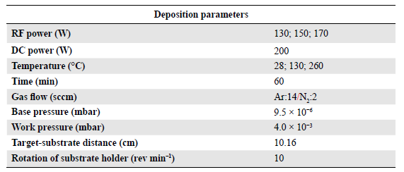
Thin films were deposited by the co-sputtering system with a Ti5Si2 target, varying the discharge power to 130W, 150W and 170W in the Zr target and to 200W in the Ti2Si5 target. Films were produced by varying the deposition temperature, starting at room temperature, 130° and 260°C.
The discharge was performed with three different powers in the RF source in order to select the power with the best results in terms of adhesion tests. The rotation speed of the substrate holder was 10rev/min, which guarantees homogeneity in the coating. The deposit parameters are observed in table 1.
Physicochemical characterization
For the SEM analysis a FEI QUANTA 200 microscope was used, in secondary electron mode, high vacuum and 30kV voltage. The qualitative chemical composition analysis was carried out using an EDS energy dispersion microprobe.
The X-ray diffraction analysis (XRD) was performed on a PanAlytical X'pert Pro equipment, with data taken at an angle of 29 between 10° and 120°, using a RTMS (realtime multiple strip) detector with Cu Kα radiation at a wavelength of 1542Å and a step size of 0.0263° in Bragg-Brentano mode.
To calculate the crystallite size, the scherrer equation D = 0.9λ / Lcosθ, was used. Where D is the crystallite size, λ is the wavelength used by the XRD source (CuKα = 1.542 Å), θ is the value of the angle at which the peak is observed and L is the full width at half maximum (FWHM).
To calculate the lattice parameter, L was used, approximating the peaks to a voight function and then using Bragg's law nλ = 2dsenθ. In this case, by taking the first order reflections with n = 1, and where d is the interplanar distance, the lattice parameter can be calculated from
 being h, k and l, Miller's index.
The morphological analysis was performed with a FEI QUANTA 200 scanning electron microscope in secondary electron mode and high vacuum with a voltage of 30 KV. The qualitative chemical composition analysis was done by means of an EDS energy-dispersion microprobe.
The thickness measurement was done on a DEKTAK 150 profilometer with 1500 μm sweep in the ridges and valleys with duration of 60 s, applying a force of 2.50 g and a resolution of 0.056 um per sample. The deposition time was one hour in order to achieve thickness of approximately 800 nm.
Mechanical Characterization
To determine the wear resistance and the coefficient of friction in one of the coatings, the tribometer used was used CERT-UMT type 2M-110, with a 6 mm diameter A12O3 alumina ball. The wear test was obtained by performing the pin-on-disk test with a speed of 10m/s and load of 1N for 600s to determine the coefficient of friction (COF). The hardness of the coating was determined by means of a Hysitron TI 950 nano-hardness kit that uses a Berkovich-type diamond indenter with a pyramidal shape at the tip and triangular base. The load used was of 5mN. For sampling purposes, 5 measurements were made randomly on the film. The indentation penetration depth did not exceed 10% of the total thickness of the substrate.
Results and discussion
Figure 2 shows the diffractograms obtained for the different deposition conditions on the Ti6Al4V substrate, with variations in power and temperature. Peaks are observed at positions 2Θ 35,125° 39,954°, 58,975° and 75,215° corresponding to the formation of the solid solution (Ti, Zr) N, which is in agreement with other research (Pogrebnjak, et al., 2012; Saladukhin, et al., 2015; Sobol, et al., 2011). Diffraction peaks increase or decrease in intensity depending on the value of the variation in the power of the RF source at 130W (a), 150W (b) and 170W (c), and on the coating deposition room temperature, 130°C and 260°C.

Figure 2 (Ti-Zr-Si)N X-ray diffractogram on Ti6Al4V substrates, at different temperatures: (a) 130W, (b) 150W and (c) 170W.
According supplementaryfigure 1,https://www.raccefyn.co/index.php/raccefyn/article/view/1198/3034, with increase of temperature, the pick (111) intensity increases too, but to increase power (or Si content), the pick (111) intensity decrease (supplementaryfigure 2,https://www.raccefyn.co/index.php/raccefyn/article/view/1198/3035). In these same numerals, it is possible to evidence a broadening of the peak, for intermediate temperatures and powers.
Some variation in the width of the peaks is observed, which can be attributed to the overlap generated by the TiN and TiZrN structures in orientation (111). This indicates a substitution of titanium by zirconium in the crystalline structure of titanium nitride (Parra, et al., 2015). Which causes the peak to appear wider, actually being the overlap of two peaks.
Some of the factors that influence the intensity of the diffraction peaks are: temperature, absorption factor, polarization factor, among others. Therefore, the width and shape of the peaks can be associated with the combination of instrumental factors and factors based on the microstructure of the sample. (Cardenas, 2018)
The intermediate position of the diffraction peaks between those of ZrN and TiN, with crystallographic charts (JC PDS 350753) and (JC PDS 381420), respectively, indicate that this phase belongs to the solid solution (Zr, Ti)N ( Sobol, et al., 2011, Cardenas, et al., 2018, Huang, et al., 2007). The other peaks shown in the figures correspond to signals typical of the substrate. In the case of coatings deposited at room temperature, they have a high intensity peak in some areas, but all reflect a crystalline microstructure.
According to (Lin, et al., 2015), the X-ray diffraction pattern for (Ti-Zr) N shows a strong orientation (111) since this is the trend to produce nitrides of the IV group of transition metals. In the analysis of the XRD samples shown in the diffractograms, there are diffraction peaks ZrN (111) and TiN (111) indicating an orientation (111). This due to the deposition conditions in which the energy deformation is dominant compared to surface energy (Benavid, et al., 2003). In addition, the development of texture (111) in thin films depends on the relationship between the energy atom and the metallic flux (Rizzo, et al., 2006) and in consequence on the partial pressure of the reactive gas, as well as on the applied discharge power. The incorporation of silicon in ZrN-based coatings increases the hardness of the films, improves the resistance to oxidation and reduces the coefficient of friction of the films (Yalamanchili, et al., 2014). The results indicate the possible FCC phase of TiN with zirconium and an amorphous phase of SiN and this forms a nanocomposite. The preferential adsorption/desorption of anions in specific crystallographic planes controls t the decrease in their surface energy (Cardenas, Raba & Rincon, 2020).
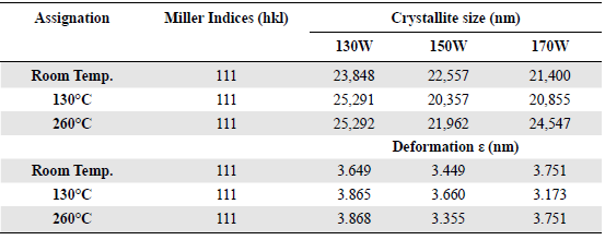
Table 2 describes the size of the crystallite for the (Ti-Zr-Si)N coating deposited on the Ti6Al4V substrate, where a change in the results is observed. This can be related to the work of (Sobol, et al., 2011), who describes that the change in the average size of the crystallites was 25nm and it can be caused by the decrease in the contents of titanium and silicon. In this case, the change was due to the power variation in the RF source directly associated with the Ti5Si2 target.
Table 2 Coating crystallite size - deformation (Ti-Zr-Si)N, substrate: Ti6Al4V, Power: 130W-150W-170W, Room Temperature: 130°C and 260°C.

The average surface roughness varies as a function of the deposit temperature of the coating according to figure 3. The roughness value increases considerably, which is in the range of 15-39nm for a power of 170W, from 10-36nm for 150W and 7-25nm for 130W. It can be concluded that there is no significant change in the roughness of the samples analyzed, since they are in an average range. This may be due to a very high efficiency in the formation of ceramic-type material. For 170W, the deposit conditions indicate a greater roughness at room temperature that decreases to 130° and 260°C. These results can be related to (Huang, et al., 2007), who describes that the TiZrN coatings show a high roughness, due to the fact that the nitrogen flow makes the Gibbs free energy selective in the formation of the Ti-Zr-N alloy, decreasing the nucleation of islands that interact in the densification of the coating. According to different properties including magnetic that are influenced by the size of the particles and the surface defects become more important as the size of the particles decreases (Cardenas, et al., 2021).

Figure 3 Roughness measurements of (Ti-Zr-Si)N coatings for Ti6Al4V substrate with RF power of (a) 130W (b) 150W and (c) 170W.
Figure 4 shows the EDS analysis at room temperature where percentages of the substrate own elements such as titanium, aluminum, vanadium were found. The presence of the deposited coating with the elements of Ti, Zr, Si and N in various amounts is evident, with a range of 43% to 47% in Titanium, 11% to 18% in zirconium and 0.8% to 2.81% in silicon. According to the work of (Pogrebnjak, et al., 2012), the chemical composition is indicated in a cross section of the (Ti-Zr-Si)N coating, which is similar with these results. The figures show the surface of the coating deposited on the alloy without pores, cracks or other defects that usually appear in the deposit. The coatings deposit had two targets for the deposit, the power variation was made through the RF source connected to the target of Ti5Si2, and a fixed value in the power of the DC source connected to the target of Zr therefore the relationship In the amount of Silicon it is directly with the variation mentioned, as well as in the values associated with titanium, it is also important to point out that the growth mechanisms of the film may vary due to the fact that not only one species is deposited from the source, In addition to this, additional processes may occur that change the characteristics of the deposit (Vanegas, Alfonso & Olaya, 2019).
Figure 5 shows the thicknesses obtained according to the power and temperature of the coatings deposit. For a power of 170W, the thickness varied between 662nm and 536nm as indicated in part (a), for 150W between 566 and 515nm (b), and finally for a power of 130W between 420 and 481nm (c). The thickness growth rate as a function of time is determined for a time of 60 minutes, where the deposit rate is 110.3A/min for a power of 170W, 94.3A/min for 150W and 80.1 A/min for 130W.

Figure 5 Thickness of the coatings according to the deposit conditions: (a) 130W, (b) 150W and (c) 170W.
The obtained results allowed to assume that due to a high power, the thickness of the film increases (greater thickness for power of 170W and less for 130W). Analysis of the coatings indicates that a thickness of the same order of magnitude is maintained for the deposited films (Cardenas, 2018). The effect of the power in the formation of the coating is favorable, specifically at 170W there is greater uniformity in the film.
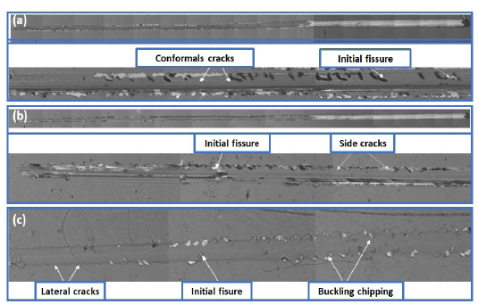
Figure 6 shows the scratch tests for Ti-Zr-Si-N coatings deposited on Ti6Al4V substrates for different temperatures and a discharge power of 170W, where thick spacing occurs and the substrate is completely exposed to the footprint left by the indenter in this case. When the diamond comes into contact with the coating at the beginning of the channel, a crack is formed at the coating-substrate interface that spreads a considerable distance before stopping. This crack may nucleate into a large interfacial defect or result in from cracking of total thickness (Kiryukhantsev-Korneev, et al., 2010).

Figure 6 Ti-Zr-Si-N film scratch footprint: (a) P = 130W - 260 °, (b) P = 150W- 260 ° C, (c) P = 170W- 260°C.
In part (a) and (b), the lateral cracks in the coating layer can be interpreted as a failure mechanism characterized by the separation of part of the layer in order to minimize the amount of elastic energy stored by the compressive efforts before the movement of the indenter.
In (c), there are conformal cracks and buckling as well as the material detached in the lateral areas. Once spallation occurs, there is a tendency for cracks to deviate from the interface to the surface, leading to extensive cracking of the coating area. During the tests, the values of Lc1 (cohesive failure) and Lc2 (adhesive failure) were determined. The cohesive failure mode consists in the separation or damage of a part of the coating and the adhesive failure that corresponds to the separation between the coating and the substrate. According to the results, the power of 170W-260°C stood out as the best deposit condition with a value Lc1 = 2.1 and Lc2 = 4.7N. These values suggest that the surface should be prepared by a nitriding process or the metallic interlayer deposit to improve the adherence of the produced systems.
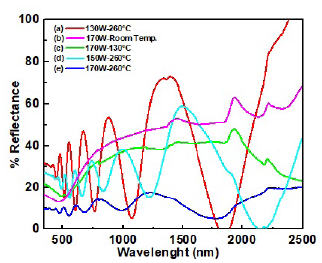
The optical reflectance spectra of the (Ti-Zr-Si)N coatings on the Ti6Al4V substrate are observed in figure 7. The results indicate that, in the infrared wavelength region, the (TiZrSi)N coating for (a) 130W-260°C has a high reflectance of approximately 72%, while for (e) 170W-260°C the lowest reflectance is registered with a value of 20%. These results are associated with the effect of temperature on the deposit of substrates. As the discharge power increases, this value decreases as shown in (b), (c), (d).

Figure 7 Experimental reflectance spectra for (Ti-Zr-Si)N coatings as a function of the wavelength of the incident electromagnetic wave: (a) 130W-260°C, (b) 170W-Room Temp., (c) 170W-130°C, (d) 150W-260°C and (e) 170W-260°C.
According to Veszelei, et al., 1994, when varying deposition parameters including the temperature of the substrate, the optical properties are different in the films obtained. A high temperature of the substrate results in a film with high optical quality, that is, high infrared reflectance and a deep minimum in the visible spectrum, as evidenced in the present work. However, these temperatures can in turn cause problems when spraying thin films, since the oxidation process accelerates with increasing temperature (Georgson, Roos & Ribbing, 1991).
The coatings produced presented high values of mechanical properties. The low values of hardness (20GPa) and elastic modulus (218GPa) were presented in the samples deposited with the lower power values (130W). This is possibly explained by an increase in the residual stresses or deformation of the structural one. The increase in the power of the discharge favors an increase in the content of defects in the film, which in turn favors structural deformation and an increase in the residual compression stresses (Olaya, Capote, & Marulanda, 2015).
The results of the COF tests and the test time are shown in figure 1S,https://www.raccefyn.co/index.php/raccefyn/article/view/1198/3033, for the sample with 130W, where COF is coefficient of friction. This was the sample that presented greater hardness and zirconium content. In these results, three regions can be observed where the value of the friction coefficient varies significantly. The first zone corresponds to times of less than 20 seconds, where a COF value close to 0.1 is observed. This result is attributed to the measurement of the tribological torque generated by the coating and the alumina ball. These low COF values can be explained by the high hardness values of the coating, the high density and by the zirconium oxide formed in the coating during its manufacturing process and/or during tribology tests (Vanegas, Alfonso & Olaya, 2019). The second part of the graph, which can be seen approximately between 20 and 150 seconds, corresponds to a transition zone that involves the gradual penetration of the indenter from the coating to the substrate. At this stage, there is loss of adhesion of the coating, generating a significant amount of particles or debris that increase the wear rates in the material. Finally, the last region of the curve is observed, after 150 seconds, corresponding to a mixed wear of the coating on the substrate. In this way, the COF value is increased to values close to 0.5, which is attributed to the reduction in surface hardness, considering that the substrate has a hardness close to 3.2GPa (Bisbal, et al., 2012).
During the wear test various wear mechanisms are generated. At the start of the test, an adhesion and sliding mechanism is favored between the surface of the alumina ball and the surface of the coating. However, with increasing time, there are a fluctuation of load and loss of coating material, which generate contact fatigue and abrasion. The increase in noise and dispersion of the COF values over time can be explained by an increase in the roughness of the surface of the coating and the in abrasive wear promoted by the debris produced between the contact surfaces. The formation of corrosive wear is probable, which explains the constant part of the COF in the final part of the test. Coating elements such as Zr, Ti and Si and Fe in the substrate can form oxides that can improve the tribological properties of the system produced over time (Macias, et al., 2019).
Conclusions
Nanostructured (Ti-Zr-Si)N coatings were deposited by means of the co-sputtering technique with variation in discharge power and deposit temperature. The XRD results indicate the formation of a crystalline microstructure with the presence of (Zr, Ti)N, ZrN and TiN, as well as peaks of the substrate. The size of the crystallite varies between 20-25nm for plane 111 and is greater for a power of 130W and a temperature of 260°C. For plane 200, the size is 13-22nm, which is greater for the power of 170W and a temperature of 260°C.
The highest roughness is observed for the power of 170W with a range of 10-36nm for the three temperatures. There is no significant change in the roughness of the samples analyzed, since they are in an average range, which may be due to a very good efficiency in the formation of the ceramic-type material. The highest growth rate for the discharge time (1h) was for 110.3A / min for a power of 170W. In the coatings analyzed by the adhesion test, adhesion failure was observed, with an RF power of 170W and a temperature of 260°C as best condition. A reflectance value of 72% was obtained for coatings deposited at 130W 260°C, which is the highest percentage. A decrease was recorded in other results, obtaining the lowest value of 20% for 170W 260°C. This is associated with the variation of the deposit parameters that generates different values in the optical properties. The coefficient of friction for the coating with the highest amount of Zr is 0.1, which can be explained by the high hardness values of these ceramic materials. The presence of silicon gives a greater hardness to the coating due to the synergistic effects of the elements present in the film with a smaller number of pores.


