


 English (pdf)
 Article in xml format
 Article references
 Send this article by e-mail
 Cited by SciELO
  Cited by Google
  Similars in
SciELO
Similars in
SciELO  Similars in Google
 Permalink
Introduction
Power electronics (PE) devices are switched systems used for the exchange or conversion of energy. Their switched nature causes ripples in voltage and current signals. Such ripples are commonly reduced by using large inductors and capacitors; however, they are not completely eliminated in the final result. In view of the unavoidable presence of ripples, PE these devices are modeled using the average value of the signal (average model), ignoring the ripple 1,2. However, applying the average model not only eliminates the ripple but also the transient of voltages and currents. The transient is fundamental since it allows to determine the extreme operating conditions of the system. Therefore, simulations must be performed to find the transient, including the dynamics of the switches and diodes which leads to a high computational burden and long simulation times.
Several applications of the average converter model are found in the specialized literature of PE converters. In 3, the modeling and control of a Floating Interleaved Boost converter (FIBC) is developed to meet the requirements of a Fuel Cell (FC) battery for vehicular applications. The average model allows reaching adequate control of the converter to improve the voltage gain and minimize the input current ripple and thus ensure the sustainability of the FC. The authors in 4 analyze the average models of nonlinear fourth-order converters operating in continuous conduction mode (CCM) to predict the frequency response. This method is based on the average model and is simpler and easier to implement than other conventional models. A detailed comparison of the CUK, D1 and D2 converters is presented in 5; using the average model, the performance of the converters is evaluated by carrying out simulations in a PV system. The authors in 6 proposed a multi-input Boost converter for renewable energy sources (RES) connected in parallel. In this case, the converter performance is maximized to maintain a constant output voltage; basically, starting from the average model, a small-signal CCM model is developed and the line-output and control-output transfer functions are derived. In 7, a PWM tapped-inductor Buck DC/DC converter is presented that aims to substantially reduce the output voltage by working with a comfortable duty cycle range and using a single-stage power converter; the average model is the basis for deriving the small-signal model to obtain the line-to-output and control-to-output transfer functions. The authors in 8 proposed a fractional order model for a Boost converter in discontinuous conduction mode (DCM), the modeling starts applying the average model of the fractional order Boost converter, and then the transfer function that relates the duty cycle with the output voltage in DCM is obtained. In 9, an equalizing converter circuit for a Half-Bridge Boost Converter operating in DCM is developed to solve the voltage unbalance that reduces the power factor. The average model is used to analyze in detail how the equalizer eliminates the voltage unbalance. The authors in 10 develop a small-signal average model of a single-stage bridgeless Boost half-bridge (AC/DC) converter with bidirectional switches using the average model. The mathematical model obtained is used to design a PI controller that proves to be stable. In 11, the transfer functions of a Buck-Boost converter are obtained using the average model of the converter. The authors in 12 present small-signal modeling for a bidirectional quasi-Z-source converter from the average model technique and provide a design guide for an AC controller for improving the stability of the converter. The authors in 13 develop modeling techniques using the average model of DC/DC converters, taking into account the non-ideal characteristics of the switching devices and improving the performance of the converters under analysis. In 14, a Luo DC-DC converter is proposed for hybrid electric vehicles. The authors perform the modeling of the converter with the state space averaging method and the average model. The authors in 15 develop a method to dynamically model the coupled-inductor Double-Boost converter. The average model of the converter is deduced to obtain the impact of the leakage inductance by using equivalent resistors.
The average model has also been widely used in PE inverters. The authors in 16 present a detailed mathematical model of a non-ideal Z-Source inverter (ZSIs) with non-minimum pase behavior to analyze the influence of the snubber capacitance using average model approaches. In 17, a multi-harmonic modeling technique for PWM-driven DC-AC inverters not ideal for low-power applications is introduced. The average model is used to anticipate the AC signal response along with the average values of the DC signal taking into account higher-order harmonic effects.
In microgrid (MG) applications, the authors in 18 discuss the droop control strategy for a voltage source inverter (VSI) in the power exchange mode with MGs or the main grid; for this, they analyze the average model of the three-phase VSI and obtain the voltage and current transfer functions. The results show that the system maintains nominal frequency and voltage. The authors in 19 develop a fuzzy logic-cyclic reports modulation control based on the average model to improve the output power quality of the single-phase series five-cell inverter. Simulation results show that the proposed control offers high performance. The authors in 20 derive the small-signal model of a three-level neutral-point-clamped inverter connected to the grid with LCL filter. The process starts with the circuit equations and the average model; finally, a control for the grid current is designed using the average model. In 21, a time domain model called harmonic average model (HM) is presented to estimate the harmonic currents generated by the inverters, In HM the superposition principle is applied to include the dead time and switching effects provided by the average model. Also, the HM is validated in wind and a photovoltaic generation. The results indicate that HM follows the references and accurately estimates the harmonic spectra. The authors in 22 develop a circulating current model based on the average model that takes into account the effects of dead time for Parallel Two-Level Three-Phase Voltage-Source Inverters.
The specialized literature extensively uses the average model in PE devices for obtaining the small signal model, which allows obtaining the stationary state of the electrical variables. Furthermore, this permits to establish control strategies and find the nominal values of PE devices in the design stage. The stationary state permits defining set points of the variables that PE devices must follow. Although the average model has multiple applications, the simulations that must be carried out to verify the dynamic behavior must include the transient in order to verify adequate stabilization times and wave overshoots; in this case, it is not possible to use the average model as it has been conventionally used since transient information is lost.
MG simulations based on power electronics devices require the transient of the signals to be captured in order to determine how the connected devices interact. In order to obtain the transient, the differential equations or the circuit implementation of the devices must be used, which leads to high computation times. In these simulations, slow and fast dynamics are obtained. The slow dynamics correspond to the transient that is given by the resistive, inductive, and capacitive values as well as the operating point, while the fast dynamics are given by the ripple of the signals that is produced by the switches and diodes. The main contribution of this paper is the application of the average model to the system consisting of the switch and diode in order to eliminate the fast dynamics (ripple) from the simulation but keep the slow dynamics. After eliminating the fast dynamics it is possible to obtain the transient of the signals using few computational resources and achieving low simulation times.
This paper is organized as follows: Section 2 presents the deduction of the average model for the Boost and Buck converter switches along with the average model of inverter switches. Section 3 compares simulations applied on a power electronics application that includes an inverter, a converter and a battery, using the proposed approach and the conventional simulation that uses power electronics switches. Section 4 concludes and highlights the most relevant aspects of the paper.
Deduction of average model for power electronics switches
The objective of this section is to derive the average model for switches and diodes of power electronics based devices. The switch model will be derived for the DC/DC Buck and Boost converters; subsequently the model will be generalized for the DC/AC inverter.
Deduction of average model for Buck converter switch
Figure 1corresponds to the Buck converter, inside the box is defined the converter switching system composed by a diode (D), and an IGBT switch (SW). The average model deduction will only be performed for the switching system, without including the passive elements (inductors or capacitors), the source, and the load. This is to eliminate the high-frequency ripple inherent to the commutation of switches and diodes but to preserve the slow dynamics inherent to the other elements of the system. In order to deduce the average model of the switching system it is necessary to define for D and SW the following: 1) the polarities of D and SW labeled as v SW and v D , respectively; 2) the current senses of D and SW, labeled as i d and i SW , respectively; 3) the input voltage (v i ) of the switching system; and 4) the output current (i o ) of the switching system. The polarities and current directions of D and SW are defined when the element is directly polarized and conducting.
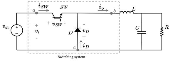
For the modeling of the switching system it is assumed that the input voltage (v i ) and the output current (i o ) are constant for each switching cycle. The switching function u is also defined such that when u = 1 the IGBT closes and the diode is reverse polarized; on the other hand, when u = 0 the IGBT opens and the diode is directly polarized.
Figure 2 a shows the switching system when u = 1. The diode is reverse polarized obtaining a voltage v D = −v i and a current i d = 0 while the switch being closed obtains a voltage v SW = 0 and the current through it is i SW = i o . Figure 2 b shows the switching system when u = 0. The diode when directly polarized obtains a voltage v D = 0 and the current flowing through it will be i d = i o ; on the other hand, the switch opens obtaining a voltage v SW = v i and a current i SW = 0.
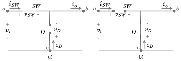
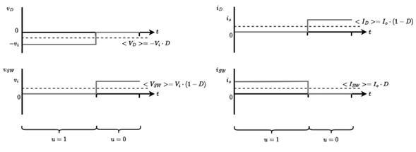
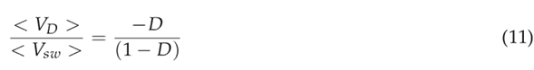
Figure 3illustrates the diode and switch voltage and current waveforms. Perfect alternation between their conduction states is assumed, i.e., no simultaneous conduction or simultaneous non-conduction is possible. The average value (in a switching cycle) of the signals is defined as follows: the average diode voltage (< V d >), the average IGBT voltage (< V SW >), the average diode current (< I d >), the average switch current (< I SW >), and the average value of the function u (D, 0 < D < 1)) corresponding to the duty cycle.
According to the above, it follows that:


Equations (5) and (6) are obtained from the division of Equation (1) with Equation (2) and from the division of Equation (3) with Equation (4).


According to Equations (5) and (6), the Buck converter switching system can be modeled with voltage and current dependent sources. Figure 4a shows the Buck converter switching system where the switch has been replaced by a voltage-dependent source and the diode by a current-dependent source. Figure 4bshows the Buck converter switching system where the switch has been replaced by a current-dependent source and the diode by a voltage-dependent source.
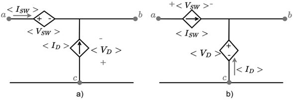
Figure 4 Buck converter with dependent current sources a) voltage and current y b) current and voltage
Note that the equivalent circuits proposed in Figure 4 allow solving the converter by means of conventional circuit analysis techniques without resorting to switching functions and neglecting the voltage and current ripple. In this way, it is possible to obtain the average transient and stationary behavior for each variable of the converter.
However, it is worth noting the assumptions that must be met for its use: a) the input voltage and output current must be constant during each switching cycle and b) there must be perfect alternation between the switch and the diode. In this case, the input voltage is related to the power supply whose value is constant (or slowly changing) in most applications. The output current is influenced by the inductor L which prevents it from changing abruptly as a result of switching. The alternating operation of the diode and switch limits the application of this model to converters operating under the continuous conduction mode.
Deduction of average model for Boost converter switch
Figure 5 corresponds to the Boost converter. The converter switching system is depicted inside the box in dashed red, which is composed by a diode (D), and a switch (SW). The deduction of the average model will only be performed for the switching system, without including the passive elements (inductors or capacitors), the source, and the load. This is done to eliminate the high-frequency ripple inherent to the switching of these elements, and to preserve the slow dynamics inherent to the other elements of the system. In order to derive the average model of the switching system, it is necessary to define for D and SW the following: 1) the polarities of D and SW, labeled as v D and v SW , respectively; 2) the current direction of D and SW, labeled as v D and i SW , respectively; 3) the input current (i i ) of the switching system, and 4) the output voltage (v o ) of the switching system. The polarities and current directions of D and SW are defined when the element is directly polarized and conducting.

For the modeling of the switching system it is assumed that the input current (i i ) and the output voltage (v o ) are constant for each switching cycle. The switching function u is also defined such that when u = 1 the IGBT closes and the diode is reversely polarized; conversely when u = 0 the IGBT opens and the diode is direct biased.
Figure 6a) shows the switching section when u = 1. The diode is reversely polarized obtaining a voltage v D = −v o and a current i d = 0 while the IGBT being closed obtains a voltage V SW = 0 and a current i SW = i i . Figure 6b) depicts the switching section when u = 0. When the diode is directly polarized its voltage is v D = 0 and the current flowing through it is i d = i i ; in this case, the IGBT opens obtaining a voltage v SW = v o and a current i SW = 0.

Perfect alternation between the diode and switch conduction states is assumed, i.e., no simultaneous conduction or simultaneous non-conduction is possible. The average value (in a switching cycle) of the signals is defined as follows: the average diode voltage (< V d >), the average IGBT voltage (< V SW >), the average diode current (< I d >), the average switch current (< I SW >), and the average value of the function u (D, 0 < D < 1)) corresponding to the duty cycle. From the above, Equations (7), (8), (9), (10) are obtained.


Equations (11) and (12) are obtained from the division of Equation (7) with Equation (8) and from the division of Equation (9) with Equation (10).

According to Equations (11) and (12), the Boost converter switching system can be modeled with voltage and current-dependent sources. Figure 7a shows the Boost converter switching system where the switch has been replaced by a voltage-dependent source and the diode by a current-dependent source. Figure 7b shows the switching system of the Boost converter where the switch has been replaced by a current-dependent source and the diode by a voltage-dependent source.
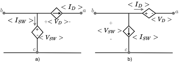
Figure 7 Boost converter with a) voltage- and current-dependent sources; and b) current- and voltage-dependent sources
Note the similarity to the deduction of the average model for the Buck converter. In this case, the constraints regarding abrupt changes are related to both, the input current and output voltage of the switching system. Sudden changes in the input current are limited by the inductor L and sudden changes of the output voltage are limited by the capacitor C.
Deduction of average model for power inverters
Figure 8 presents a bidirectional DC/AC inverter which is composed of a DC voltage source (v dc ), an AC voltage source (v ac ), two capacitors (C 1) and (C2), an inductor (L), two switches (SW 1) and (SW 2) and two diodes (D 1) and (D 2).

The inverter has two operating modes: 1) In operating mode 1, the source and DC bus deliver power to the AC power system, in this operating mode the inverter delivers at the AC terminals a lower voltage with respect to the DC bus voltage. 2) In operating mode 2, the power system delivers power to the DC bus, in this operating mode the inverter increases the voltage at the DC terminals with respect to the inverter’s AC voltage. The modes of operation are described below.
Mode 1: Power inverter working as DC-AC converter
In this mode of operation, the power flows from the DC bus to the power system. The inverter operates using the same semiconductors or topology of the Buck converter. The switches to be activated in this mode are SW 1 and D 2. Note that Figure 9a, corresponds to the same topology of the Buck converter in Figure 1. Figure 9b results after replacing the controlled voltage and current sources in Figure 4a.
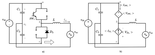
Figure 9 Inverter operation as DC-AC converter mode: a) switching state, b) model using voltage and current controlled sources
Using Equations (5) and (6) and being
 it follows that:


2.5. Mode 2: Power inverter working as AC-DC converter
In this operating mode, the power flows from the power system to the DC bus. The inverter operates using the same semiconductors or topology of the Boost converter. The switches to be activated in this mode are SW 2 and D 1. Note that Figure 10a, corresponds to the same topology of the Boost converter in Figure 5. Figure 10b results after replacing the controlled voltage and current sources in Figure 7b.
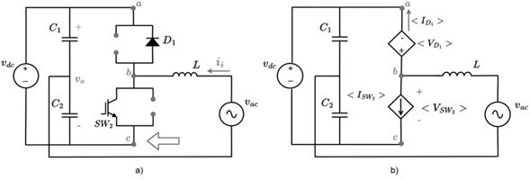
Figure 10 Inverter operation as AC-DC converter mode: a) switching state, b) model using current and voltage controlled sources
Using Equations (11) and (12) and being  it follows that:

Note that the circuit model of controlled voltage and current sources at terminals a,b, and c for operating mode 1 (Figure 9b) and operating mode 2 (Figure 10b) have the same structure. Note also that the model Equations governing the controlled sources for operating mode 1 (Equations (13) and (14)) and for operating mode 2 (Equations (15) and (16)) are the same. Observing the circuit model together with the equations model for both operating modes it can be seen that both models are equivalent; therefore, it is possible to simplify the two modes of operation into a single one and therefore model the inverter switch with a single controlled current source and a single controlled voltage source.
Simulation results
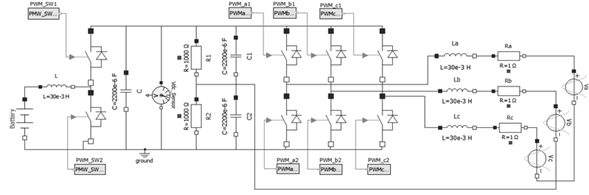
Figure 11 shows the system under study which is composed of a battery, a bidirectional DC/DC converter and a three-phase DC/AC bidirectional inverter connected to the power grid. The battery has a nominal voltage of 48V. Next is the DC/DC converter which is composed of an inductance L = 30mH two pulse width modulated (PWM) switches and a capacitor C = 20µF. Next is the inverter which is made up of two balancing resistors R 1 = R 2 = 1000Ω, two capacitors that make up a DC bus C 1 = C 2 = 2200µF, six sinusoidal PWM (SPWM) and the inductances L a = L b = L c = 30mH and resistors R a = R b = R c = 1Ω that connect to the electrical network considered as V a = V b = V c = 120 V AC at 50Hz.
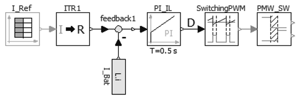
The battery current control is carried out by the closed-loop control illustrated in Figure 12. The difference between the reference current I Re f and the battery current I Bat is fed to the PI I L controller which has an integral time of Ts = 0,5s and a gain K = 0,01. In this way, the control signal D is obtained. Finally, the Dsignal is compared with a triangular signal using the SwitchingPWM block to obtain the periodic signal that is applied to the converter switches. To avoid the two converter switches to be closed at the same time, the dead time given by the PWM SW block is used. The value of the reference current at t = 0s is I Re f = 30A and at t = 2s is I Re f = −50A.
Since the three-phase DC/AC inverter has non-minimum phase, it is necessary to use a cascade controller to control the DC bus voltage made up of C 1 and C 2. Figure 13 shows the implemented control strategy which uses the dqz transform to the inductor currents L a , L b and L c through the SW con block. This gives the current I d which guarantees the active power flow and I q which guarantees the reactive power flow. Thus, current I d is needed to control the DC voltage of capacitor C and current I q d to control the reactive compensation of the system.
The DC bus voltage control consists initially in obtaining the difference between the reference voltage V Re f and the DC bus voltage V DC measured by the Vdc Sensor sensor in Figure 11. Then, this difference is taken to the PI Vdc controller which has an integral time Ts = 0,019s and a gain K = 0,335. The resulting control signal is compared to the current I d and the difference is taken to the PI d controller which has a time integral Ts = 0,00012 and a gain K = −1,8054. The result is the control signal for the capacitor voltage C at dqz. The reference voltage value at t = 0s is V Re f = 610V and at t = 1,3s V Re f = 615V.
To compensate the reactive current of the system, the difference between the reference current Iq Re f and I q is made. This information is given to the controller PI q which has an integral time of Ts = 0,00011s and a gain K = −1,68069. This provides the control with the signal for reactive current compensation at dqz.
The control signals obtained are transformed with the inverse transform of dqz and the signals A, B, C are obtained. These sinusoidal signals are normalized and an offset is added in the blocks Da, Db, Dc; this to obtain positive signals that can be compared by the SwitchingPWM blocks and subsequently introduce dead time for each pair of switches of the three branches of the inverter.
Figure 14shows the system under study applying the proposed average switch model. Note that the switches have been replaced by voltage and current-dependent sources and the equations of these sources correspond to the equations of the average switch model.

The battery current control of the system under study using the proposed model is illustrated in Figure 15. The control is performed in the same way as developed for the system with switches but differs in that the control signal obtained from the controller PI IL is used directly in the equations of the dependent sources of the DC/DC converter as the duty.
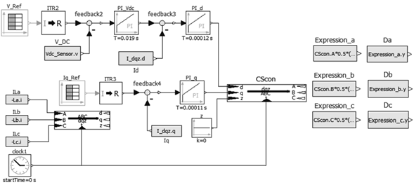
Figure 16 illustrates the control strategy for the DC bus voltage and reactive current compensation. The control is performed in the same way as developed for the system with switches but differs in that the signals D a , D b and D c are used as the duty in the equations of the controlled sources of the invertir switches.
The two simulations were performed in OpenModelica version 3.2.3 on an OPTIPLEX 5090 Intel Core i7-10700 @2.9GHz with 16GB RAM and 64 bit operating system. The simulation times are presented in Table I. The switched simulation takes 473.3 times longer than the average model simulation. That is to say, the proposed approach allows a 99.78 % of simulation time reduction.
Subsection

Figure 17shows the time dynamics of the battery voltage. The continuous blue signal
 is the voltage obtained from the switched model and the dotted pink signal
 is the voltage obtained from the proposed average model. It is observed that initially the battery has 48V at t = 0s, then the battery starts to deliver power to the grid and the first transient occurs where there is a small difference between
 and
and
 . On the other hand, at t = 2s the battery starts to absorb energy from the grid, it presents a second transient where there is no much difference between
 and
and
 compared to the first transient. Finally, a steady state is shown where both
 and
and
 converge to the same value.
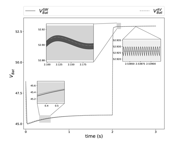

Figure 18 shows the time dynamics of the current in the battery. The solid green signal I
REF
is the reference current, the solid blue signal
 is the current obtained from the switched model and the dotted pink signal
 is the current obtained from the proposed average model. Initially, at t = 0s, I
REF
indicates a positive current of 30A meaning that current is flowing from the battery to the grid; then at t = 2s, I
REF
changes to a negative current of −50A indicating that it is flowing from the grid to the battery. In the first transient state illustrated it can be observed the difference between the
is the current obtained from the proposed average model. Initially, at t = 0s, I
REF
indicates a positive current of 30A meaning that current is flowing from the battery to the grid; then at t = 2s, I
REF
changes to a negative current of −50A indicating that it is flowing from the grid to the battery. In the first transient state illustrated it can be observed the difference between the
 and
and
 signals while in the second transient state the difference between these signals is considerably less. Both
 and
and
 signals converge to the reference value I
REF
in the steady states.
signals converge to the reference value I
REF
in the steady states.
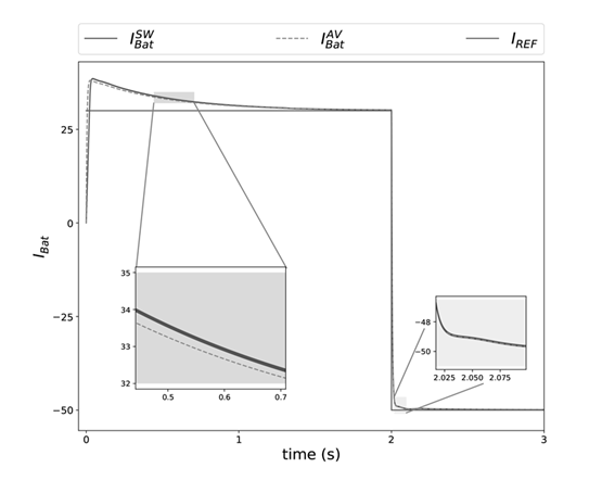
Figure 19 shows the time response of the controlled voltage on the DC bus of the system under study. The green continuous signal V
REF
represents the reference voltage, the blue continuous signal
 represents the voltage obtained using the switched model and the pink dotted signal
 represents the voltage obtained using the average model. At t = 0s the V
REF
signal indicates a DC bus voltage of 610V, then at t = 1,3s the V
REF
signal changes to 615v on the DC bus. The first two transients (t = 0s, t = 1,3s) observed occur due to the change in the V
REF
signal, while the third transient t = 2s occurs due to the change in the I
REF
signal at the battery (see Figure 18). It can be observed that in the first transient there is a difference between the
represents the voltage obtained using the average model. At t = 0s the V
REF
signal indicates a DC bus voltage of 610V, then at t = 1,3s the V
REF
signal changes to 615v on the DC bus. The first two transients (t = 0s, t = 1,3s) observed occur due to the change in the V
REF
signal, while the third transient t = 2s occurs due to the change in the I
REF
signal at the battery (see Figure 18). It can be observed that in the first transient there is a difference between the
 and
and
 signals; on the other hand, in the following transients no comparable difference is seen between these signals. Before the different changes, the
 and
and
 signals reach the reference value in the steady states and present a similar settling time.
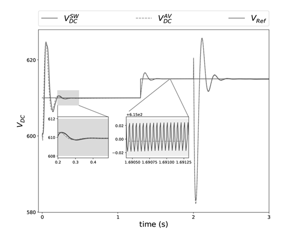
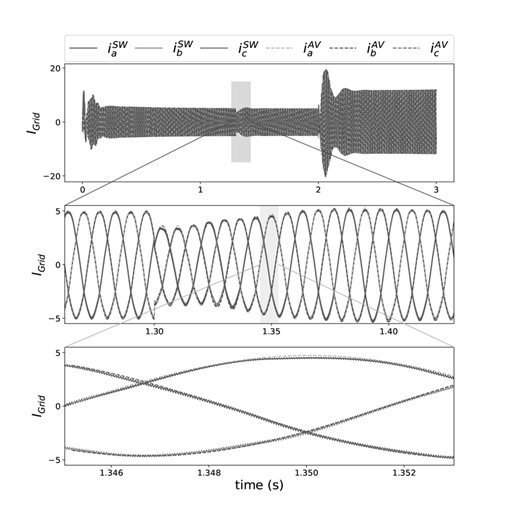
Figure 20 shows the three-phase grid currents provided by the inverter of the proposed system. Shown in blue, pink and green solid line are the
 currents obtained under the switched model and in yellow, purple and red dotted line are the
 currents obtained under the average model. Three disturbances can be observed; the first one is due to the change in voltage V
REF
= 610V of the DC bus and the change I
REF
= 30A of the battery at t = 0s. The second disturbance is caused by the voltage change V
REF
= 615V of the DC bus at t = 1,3s, the three-phase current presents a transient and stabilizes again without changing its amplitude. And finally, the third disturbance is due to the change in I
REF
= −50A at t = 2s, this time as the battery is absorbing energy, the amplitude of the three-phase currents increases considerably. Before the different changes, the three-phase currents obtained by the switched model and the average model reach the steady state maintaining the 120º phase difference between them.
currents obtained under the average model. Three disturbances can be observed; the first one is due to the change in voltage V
REF
= 610V of the DC bus and the change I
REF
= 30A of the battery at t = 0s. The second disturbance is caused by the voltage change V
REF
= 615V of the DC bus at t = 1,3s, the three-phase current presents a transient and stabilizes again without changing its amplitude. And finally, the third disturbance is due to the change in I
REF
= −50A at t = 2s, this time as the battery is absorbing energy, the amplitude of the three-phase currents increases considerably. Before the different changes, the three-phase currents obtained by the switched model and the average model reach the steady state maintaining the 120º phase difference between them.
Conclusions
This paper presents the deduction of the average switch model for PE devices in order to reduce simulation times. Ripple was eliminated from the simulation; nonetheless, voltage and current transients are preserved which allows determining the low behavior dynamics of PE devices. Several simulations using both the conventional switch-based model and the proposed average switch model were performed using OpenModelica software. In this case, a system consisting of a battery, a DC/DC converter and a grid-connected inverter was used for validating the applicability and effectiveness of the proposed average switch model.
By comparing the switch-based model with the proposed average switch model, it is observed that voltage and current for both models match quite well, the signals of the average model correspond to the signals of switch-based model conserving the transient behavior but eliminating the ripple. It is very important to point out that the simulated system is composed of AC and DC power interfaces such as inverters and converters but also batteries that introduce other types of non-linearities in the system. In other words, a wide range of PE devices was included in the simulation.
Simulation times were substantially reduced. The simulation using the switch-based model took 386.284 seconds, while the simulation using the proposed average model took 0.816 seconds. This represents a reduction time of 99.788 %. It can be concluded that applying the average model to the switch in PE devices is an alternative that allows to simulate while preserving the low dynamics of the system, with an important reduction of the simulation time, which opens the possibility to simulate more complex systems such as microgrids or other complex PE systems using home or office computers

