


 Inglés (pdf)
 Articulo en XML
 Referencias del artículo
 Enviar articulo por email
 Citado por SciELO
  Citado por Google
  Similares en
SciELO
Similares en
SciELO  Similares en Google
 Permalink
INTRODUCTION
The radioelectric spectrum is not being used efficiently. The main reason for this is that frequency bands are assigned to primary users (PU), which do not allow any other service to use their bands, even though they are only used occasionally [1]. An example of misuse of the spectrum are television bands: Those ones are not being used anymore for analog television transmission, therefore they are in a re-licensing process for digital TV [2] and WRAN services [3].
The main goal of cognitive radio (CR) is to provide an RF system capable of knowing its environment and adjusting its parameters accordingly [4]. This is a promising solution for the misuse of the radioelectric spectrum in the next years. One of the most important components of a CR is the spectrum sensing function, which detects spectral holes and primary users in the environment. This information is then used by the radio system to decide which band to use and transmit the data.
Preliminary work on cognitive radio (CR) focused on its technology modeling, simulation, and implementation. Its main issues consider three levels: Spectrum sensing [5][6][7], spectrum access [8], and hardware implementation [5]. So, the current trends in ultra-wideband wireless communications have increased the complexity of the CR systems, particularly its hardware receivers.
Some studies investigating CR have been carried out on hardware experiments and prototypes, focusing in spectrum sensing techniques such as analog-to-information converters (AIC), modulated wideband converters (MWC), and multi-coset samplers (MC).
Many approaches have been proposed on designing and implementing AIC subsystems, such as theories and simulations where the demodulation, as well as the mixer components, define the primary design specifications. A transistor-level simulation for an AIC is described in [9], which uses a mixer based on a Gilbert cell and CMOS 0.13μm fabrication technology, achieving a sampling frequency of 100 MSample/s. On the other hand, [10] presents a behavioral model which considers the dominant parameters for a detailed design to implement an AIC, with a bandwidth of 40 MHz. In [11], the authors present a working prototype of AIC, which is based on a commercial digital signal processor (DSP) board that has a clock frequency of 160 MHz; however, the AIC bandwidth is 400 kHz. Very-large-scale integration (VLSI) design level allows to research also for implementation parameters of AIC with this technology: In this regard, [12] presents a VLSI design of an AIC with CMOS 28 nm fabrication technology, which can sample RF signals up to 6 GS/s. In [13], the authors present an AIC built with integrated circuits (IC), which can sample signals with a bandwidth of up to 236 MHz: Its design specifies a printed circuit board (PCB), a commercial IC, and a chipset designed with 0.45 (im InP HBT (Indium-Phosphide heterojunction bipolar transistor) technology.
Regarding the MWC subsystems, there are three relevant works related to hardware implementation. A recent contribution of [14], concerning to a hardware prototype, proposes a system based on a FPGA, a commercial ADC, and environments such as Matlab and Labview; it has an unknown total bandwidth occupancy of up to 200 MHz and Nyquist rate of 6 GHz. On the other hand, a doctoral thesis developed at Stanford University [15] presents the VLSI implementation of an MWC receiver, which is able to detect four 1.4 MHz channels up to 900 MHz. Finally, in [16] the authors describe the Xampling platform based on MWC with support to sample signals with 2 GHz Nyquist rate, 120 MHz spectrum occupancy, and a sampling rate of 280 MHz.
Regarding MC-based sampling systems, the main findings show how it has gained popularity. A MC sampler prototype based on discrete integrated circuits is presented in [17], where an FPGA can sample signals with a bandwidth of 100 kHz and 10 sampling channels. In [18], the authors present an implementation of a MC-based sub-Nyquist sampling scheme for a surveillance radar with 1. 1 GHz bandwidth; however, no details of the hardware implementation parameters are offered. Moreover, an algorithm for broadband spectrum sensing based on sFFT is presented [19], which uses two sampling channels: Its implementation was carried out by using the software-defined radio (SDR) platform USRP [15], with a bandwidth up to 900 MHz. In [20], an algorithm to perform cooperative wideband spectrum sensing (and its hardware implementation) is presented, based on MC sampling: It is robust to noise, overcoming the performance of the algorithm presented in [19]. On the other hand, another doctoral thesis is presented by the Georgia Institute of Technology [19], which describes an asynchronous multi-rate sampling system, similar to the MC sampling: Its hardware implementation can achieve a bandwidth up to 18 GHz.
Recent evidence suggests that CR receivers can monitor wide spectra by sampling at very low rates, such as [21], which the authors describe as "the first hardware implementation results", achieving a sampling frequency of 200 MHz and resolving an instantaneous bandwidth of 2GHz by using two ADCs, an FPGA demo board, and other commercial integrated circuits.
As for complete testbed implementations for CR, all the studies reviewed so far suffer from the commercial availability of implementations about sub-Nyquist sampling systems, especially as testbeds for the academic and scientific community. Nevertheless, the embedded platform BEE2 (Berkeley Emulation Engine 2, developed at the University of California) for high performance computing is presented in [22] as a framework with 5 high performance FPGA, for designing high-end reconfigurable and complex computers. This platform was used by [23] to implement a spectrum sensing system, however, this is not based on sub-Nyquist sampling. On the other hand, an FPGA-based platform, called CRUSH by the authors [24], was conceived as a testbed for spectrum sensing systems. CRUSH is also based on the SDR platform USRP [25], and only supports NSS (Narrowband Spectrum Sensing).
Considering that testbeds are very useful tools to assess the performance of different CR algorithms and techniques, and the fact that many authors offer no explanation about the detailed design for the hardware implementation and electronic support systems, the main contribution of the work presented in this paper is a configurable testbed with the necessary circuits to capture real wireless signals by using sub-Nyquist sampling. Hence, our system would be at the same level as the ones implemented at Israel Technology Institute and California University [22][26]. In addition, this testbed would allow students to make different experiments with cutting-edge technology communication devices, to change configuration parameters for tuning the system, or testing new algorithms. Finally, remote access to our testbed opens the door for collaborative work between various universities, and thus it could have a greater impact in the academic community.
The paper is organized as follows: Section 1 describes the testbed architecture, starting with the RF system and analog frontend, the hardware/firmware configuration for the SOC-FPGA, and the information system. Section 2 presents the experiments performed to the testbed: Verification results for both the analog frontend and the SOC/ FPGA system, and tests for the web server. In Section 3, a conclusion is drawn, and acknowledgements are given in Section 4.
1. TESTBED ARCHITECTURE
In this section, different components of the sensing platform are described, starting with the RF components (antenna, and RF interface). After that, the analog front end between the RF sub-system and the SOC-FPGA will be presented. The chapter ends with the description of the information management service for the spectrum sensing platform.
1.1 RF System
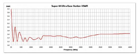
An antenna that would allow to capture wideband signals in the UHF frequency range (between 300 MHz and 3 GHz) with a good gain was needed. The M-Series Ultra Base Station antenna [27] was a great option for our requirements, since it covers the frequency range from 25 MHz to 6 GHz in obstructed non-line-of-sight (NLOS) environments, and it has omnidirectional detection. shows the Voltage Standing Wave Ratio (VSWR) for the Super-M Ultra Base Station antenna: It is lower than 2.0 from frequencies greater than 25 MHz, making detection possible for this frequency range [27].
For the radio frequency (RF) interface, an analog system that did not limit our bandwidth with a built-in low pass filter (LPF), like most commercial devices, was needed. Hence, the Myriad RF board [28] was selected: It is a low cost universal radio development platform, based on LMS6002DFN transceiver (). This board can receive incoming signals between 0.3 and 2.8 GHz, and down-convert them to baseband with a bandwidth of 14 MHz in normal operation. This board allows the developer to bypass the built-in lowpass-filters with a simple configuration, and to increase the bandwidth to 95 MHz.
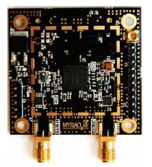
This board has two SMA connectors for the antenna interface, and it is equipped with pin headers for power supply, reference clock, analog I/Q input/output, and SPI interface connections. It contains everything needed to connect it with baseband chipsets or FPGAs, allowing the user to set parameters such as central frequency, gain, bandwidth, or sampling rates.
1.2 Architecture of Designed AIC
An Analog-to-Information Converter (AIC) based on Random Demodulator (RD) was designed by using block diagram in [29] [9].

In , x(t) is a signal which is representable and compressible in Fourier basis; ψ/ n (t) = e jωnt ); p c (t) is a pseudo-random square wave with chipping rate of BW Hz, where BW is the bandwidth of x(t); and h(t) is the impulse response of an anti-alias low-pass filter. Then, Spectral Reconstruction block has to solve the Compressed Sensing (CS) problem stated in equation (1).

Where à Є ℂ N is the estimated sparse vector, y Є ℂ M is the vector containing the sub-Nyquist samples, and È Є ℂMxN is the measurement matrix which is computed according to equation (2).

Designed AIC can recover signals with BW=100 MHz by using a sub-Nyquist rate of R=4 MHz, which leads to a downsampling ratio of N/M=25. It was implemented by using off-the-shelf analog components and a SoC FPGA-based board. In this case, mixer and anti-alias filter were constructed by using an integrated Gilbert cell and a first order low-pass filter, respectively. On the other hand, generation of , analog to digital conversion, and spectral reconstruction were implemented by means of the ADC-SoC board, by taking advantage of both FPGA and HPS portions of Cyclone V chip [30][31].
Mixer circuit performs multiplication of x(t) and pc(t), and it was implemented by using a Gilbert cell built from the HFA-3101 high-speed transistor [32]. shows designed Gilbert cell.

In, biasing circuit was not included for the sake of simplicity [32]. Nonetheless, to perform mixing, x(t) and p c (t) are required to be low voltage differential signals, since mixer has an approximate gain of 12 x. In addition, to feed compressed signal into ADC in ADC-SoC board, it is necessary to convert the differential signal from mixer output to single-ended, and to perform low-pass filtering. Both operations were accomplished by using circuit in.

Source: Prepared by the authors.
Figure 5 Circuit for Differential to Single-ended Conversion and Low-pass Filtering
Circuit in was built from the operational amplifier ADA-4807 [33], where conversion from differential to single-ended is performed with unity gain, and the output stage is a first-order low-pass filter with transfer function given in equation (3).

From equation (3) it can be observed that cut-off frequency of filter is f _c ≈ 2 MHz, therefore sub-Nyquist rate can be up to R=4 MHz. Finally, DC-blocking capacitors were used to isolate bias from mixer.
SoC-FPGA chip was used to implement the digital sub-system of designed AIC. FPGA-side was used to manage ADC and to generate a PN sequence, and HPS-side was used to manage circuit on FPGA and to execute spectrum recovery algorithms. shows the implemented circuit on FPGA-side.
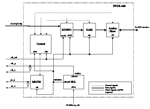
Circuit in is composed of six systems: Phase-Locked Loop (PLL), Maximal Length Linear-Feedback Shift Register (MLFSR), Dual Clock First In First Out (DCFIFO) circuit, on-chip Random Access Memory (RAM), Avalon slave [34], and Control Circuit. PLL is used to generate two clock signals of 100 MHz and 4 MHz; 100 MHz clock signal is used for synchronization of MLFSR, DCFIFO, on-chip RAM and HPS-To-FPGA interface [31]; and 4 MHz signal is used to synchronize external ADC chip. MLFSR is 9-bit wide, and uses primitive polynomial in p(x) = x9 + x5 + 1 [35] to generate PN sequence. DCFIFO allows transfer of samples from ADC to on-chip RAM by using two clock domains. Avalon slave serves as gateway between FPGA-side and HPS-side, through which HPS can start a capture operation and read acquired sub-Nyquist samples. Finally, Control Circuit manages operation of AIC by using one 4-state Finite State Machine (FSM), whose ASM chart is shown in .

FSM operates along with three counters lat_cnt, rd_cnt, and wr_cnt; five flip-flop synchronizers for clock domain crossing; and one combinational circuit to control write operations of on-chip RAM. Operation of FSM is described as follows: In IDLE state, FSM waits for a capture operation, which is triggered when start=1. Then, it enters into Latency state, where it enables MLFSR and waits for 12-cycle latency of AD9254 ADC [36] by using lat_cnt: This ensures synchronization between p c (t) signal and captured vector for proper RD operation [9] [37]. Once latency passes, FSM enters into Capture state, where samples from ADC are written into DCFIFO as long samples from DCFIFO are written into on-chip RAM: This operation is controlled by means of rd_cnt, wr_cnt, and is_fifo_rdempty flag from DCFIFO. Finally, capture end is signaled by doneflag in DONE state, after which FSM returns to IDLE state.
Regarding software for our AIC implementation, irst we wrote a C program to achieve low level access to FPGA-side hardware through HPS-To-FPGA interface, and retrieve vector y from RD. Then, we made a Python implementation of spectrum reconstruction algorithm Compressive Sampling Matching Pursuit (CoSaMP) to solve the CS problem in equation (1) [38].
1.3 Information Management Service
We designed and implemented a web application to manage the testbed data. This app allows the users to observe the captured spectra for configuring different parameters like bandwidth or central frequency, and for uploading different sensing algorithms to the embedded system.
The information management service has two main components: The web server, and the embedded sensing client. The main architecture of this system is shown in.

The functioning parameters for our system to work correctly are listed below:
32768-points spectra storage capacity.
Easy visualization/download of historical data.
Capable of uploading different sensing algorithms to the embedded sensing client.
Ability to configure different parameters such as central frequency, bandwidth, capture period and spectral resolution.
Compatible with the embedded system technology.
It was decided to use Python to develop both the web server and the embedded sensing client, for its compatibility with web applications and embedded systems [39]. A web server was implemented to interact with the human users and the embedded sensing client. In this regard, it was decided to use Flask [40], a Python framework used in web applications development, to implement our server.
The web server has four main tasks: Two of them are oriented to the interaction with the human client, and the others are focused on the embedded sensing client. The web server tasks overview is presented in.

All of the data needed by the web server are stored in a database with three tables: The first one is used to store the spectrum data, the second one is used for the configuration parameters, and the third stores the human user's information. Also, every spectrum captured by the embedded platform is stored, along with another intrinsic parameters such as central frequency, bandwidth, frequency resolution, and timestamp. All the frequency components are stored as a text string separated by commas. shows the spectrum table of the database.
Table 1 Spectrum Table for the Web Server Database
| Spectrum | |
|---|---|
| ID | INTEGER |
| DFT | MEDIUMTEXT |
| Central frequency | INTEGER |
| Bandwidth | INTEGER |
| Frequency resolution | INTEGER |
| Timestamp | TIMESTAMP |
Source: Prepared by the authors.
The configuration parameters must stay still, unless someone changes them; for that reason, they are stored in another table of the database. These data are overwritten every time someone updates any parameter. The member "Pending updates" is used as a flag to check if the current sensing algorithm is up to date in the embedded system or not. shows the configuration data table of the database.
Table 2 Configuration Data Table for the Web Server Database
| ConfigData | |
|---|---|
| ID | INTEGER |
| Central frequency | INTEGER |
| Bandwidth | INTEGER |
| Frequency resolution | FLOAT |
| Capture period | INTEGER |
| Current algorithm | MEDIUMTEXT |
| FFT points | INTEGER |
| Pending updates | MEDIUMTEXT |
| timestamp | TIMESTAMP |
Source: Prepared by the authors.
The last table of our database is used to store basic information of the web application users. This information is used to demand a login of the user before he or she updates any configuration parameter and, therefore, to have some control over who can access the system. Stored information of human users is shown in . The login password is hashed before it is saved (using SHA-256), so the security of the users is not compromised.
Table 3 User Data Table for the Web Server Database
| Spectrum | |
|---|---|
| ID | INTEGER |
| Username | MEDIUMTEXT |
| Password | MEDIUMTEXT |
| MEDIUMTEXT | |
Source: Prepared by the authors.
The web server has a graphic user interface (GUI) to interact with the human clients using a web browser. It was developed using mostly HTML, but we some Flask utilities were also used to implement the web forms.
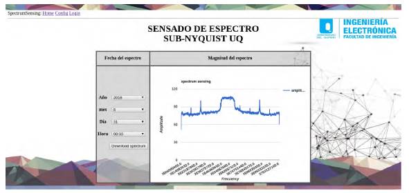
The main page of our interface allows the client to see or download every spectrum captured by the embedded sensing client. The plotted spectrum data must be selected by date, starting by the year and inishing by the hour in which they were captured. shows the GUI for the spectrum sensing visualization. This information can be accessed by anyone interested without restriction, and every single spectrum captured by the sensor can be downloaded in CSV format and imported from Matlab.

Other important page in our web application allows the user to change the configuration of the embedded sensing client using a simple user interface. The configuration page shown in permits the user to change the central frequency, desired bandwidth, spectral resolution, sensing period, and spectrum sensing algorithm.

Source: Prepared by the authors.
Figure 11 Spectrum Sensing Configuration GUI for the Web Application
Every user must be logged in before he or she can change any of the parameters shown in . This action is performed in the login page, shown in. This page allows the user to create an account if he or she does not have one already.

Embedded platform performs spectrum sensing by means of a Python program that constantly sends every spectrum captured to the web server. This program also updates the sensing parameters and sensing algorithms using polling synchronization, which allows the embedded client to work correctly from anywhere in the world without having a public IP, just an Internet connection to communicate with the web server.
There are two periodic Python tasks running on the embedded platform using timers. The first one updates the sensing parameters, and the second one obtains the current spectrum and sends it to the web server. Both algorithms are shown in.
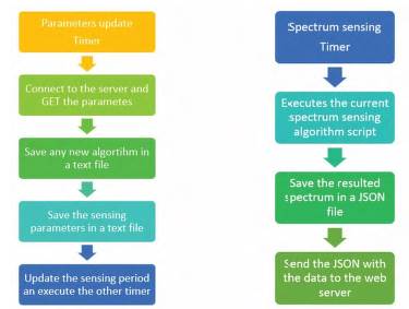
The parameter update timer is executed every 2 seconds. In every iteration, it requests the current parameters and saves them into a text file. The spectrum sensing timer is executed periodically, depending on the sensing time parameter. Each time the spectrum sensing timer is triggered, it asks FPGA for the current spectrum, then saves it in a JSON format, and sends it to the web server.
2. TESTBED VERIFICATION RESULTS
This section describes a set of tests that were performed to prove the correct operation of the built testbed and its sub-systems. First, AIC to verify the spectrum recovery of sparse signals; after that, the spectrum monitoring capabilities of testbed were verified, and finally, responsiveness of server to clients was measured.
2.1 AIC verification results
Designed AIC was tested by using a measurement window of 125 us, which leads to values for M and N of 500 and 12500, respectively. In addition, a multi-tone signal with frequencies of 4.17 MHz, 14.19 MHz, 25.02 MHz and 35.36MHz was used as a test vehicle. This signal was fed into the AIC, and then M=500 samples were acquired and stored in y vector.
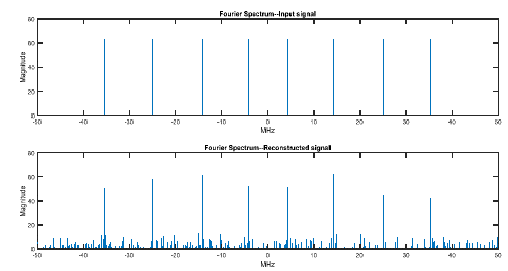
Top of shows spectrum of test signal and bottom shows recovered spectrum when using CoSaMP algorithm. Results in show that CoSaMP did it well recovering support of a: This can be verified when calculating average squared error, which amounts to 0.0005897302. Hence, this well-known algorithm was able to perform spectral reconstruction from samples acquired by our mixed-signal hardware.
Finally, shows synthesis results for the FPGA-side circuit in when implemented on the Cyclone V device of ADC-SoC board [30][31]. Results in demonstrate that digital hardware for designed AIC fits on a low-end SoC-FPGA chip, providing a complete low-cost sub-Nyquist sampling solution for compressible signals.
Table 4 Synthesis Results of AIC Hardware
| Parameter | Value |
|---|---|
| Adaptive Logic Modules | 1959 / 15880 (12 %) |
| Dedicated Logic Registers | 2445 / 31760 (8 %) |
| Block Memory Bits | 1628672 / 2764800 (59 %) |
| PLLs | 1 / 5 (20 %) |
| Operating Frequency (MLFSR clock) | 125 MHz |
| Operating Frequency (ADC clock) | 300 MHz |
Source: Prepared by the authors.
2.2 Spectrum monitoring capabilities
The testbed can perform spectrum monitoring around any frequency of UHF band with an instantaneous bandwidth of 100 MHz. This allowed to perform a large amount of measurements on this band; however, these results were narrowed down to demonstrate the correct operation of testbed.

Source: Prepared by the authors.
Figure 15 Spectrum for Colombian HD-TV Channels Caracol (473 MHz) and RCN (479 MHz)
shows spectrum measurement around frequency 473 MHz, where two Colombian HD-TV channels reside. From this it is possible to observe two typical DVB-T2 spectral shapes, corresponding to TV channels Caracol (473 MHz) and RCN (479 MHz), whose spectrum occupancy could be monitored by using our testbed [41].
Shows spectrum measurement around frequency 2655 MHz, where Long Term Evolution (LTE) downlink in band 7 resides [42], in this case, for carrier Claro in Colombia. The figure also depicts a typical LTE spectral shape for a channel with 15-MHz bandwidth [42].
2.3 Web server traffic tests
The web server described in section 1 can be used by many people around the world to experiment with different sensing algorithms, and to observe the historical spectral data. Nevertheless, the web application is not aimed at handling high traffic or hundreds of requests at the same time. Some tests were performed using the Jmeter software [43] to analyze the performance of the web server when executing the following tasks:
Watching spectral data is the most demanding task of the web server because it must find the desired spectrum (32.768-long) in the database according to the selected date, retrieve it to the browser, and plot it. Two experiments were performed to test the latency of this task. In the first one, there was only one client requesting the data 300 times. In the second one, 10 simultaneous clients were configured, each of them requesting 30 plots. Results of both experiments are shown in , which shows that the latency of the web server is a little higher than 8 seconds when 10 users are trying to watch the spectral data at the same time. If only one person is accessing the application, the latency is reduced to 0.86 seconds.
Table 5 Performance test for plotting spectral data.
| #samples | Avg. | Min. | Max. | Std. Dev. | Error % | Throughput | Received kB | |
|---|---|---|---|---|---|---|---|---|
| 1 client | 300 | 860 | 829 | 1033 | 21.38 | 0.00 % | 1.2/sec | 2542.76 |
| 10 clients | 300 | 8471 | 881 | 9498 | 875.62 | 0.00 % | 1.1/sec | 2484.51 |
Source: Prepared by the authors.
The performance of the web server when logging in and updating the sensing parameters for the spectrum sensing was also tested. Therefore, tests were performed for one user performing 500 operations, and 10 simultaneous users performing 100 operations each ( ).
Table 6 Performance Test for Log in and Updating Parameters
| #samples | Avg. | Min. | Max. | Std. Dev. | Error % | Throughput | Received kB | |
|---|---|---|---|---|---|---|---|---|
| 1 client Logging in | 500 | 52 | 49 | 86 | 3.87 | 0.00 % | 16.6/sec | 70.73 |
| 1 client Upd. params | 1000 | 7 | 6 | 26 | 1.3 | 0.00 % | 33.2/sec | 136.21 |
| 10 clients Logging in | 1000 | 309 | 51 | 448 | 46.89 | 0.00 % | 17.1/sec | 73.05 |
| 10 clients Upd. params | 2000 | 265 | 8 | 407 | 46.64 | 0.00 % | 34.2/sec | 140.47 |
Source: Prepared by the authors.
Shows that this operation is a lot faster than watching spectral data, since it only takes about 52 ms to login one client, and 309 ms when ten clients are trying to do so at the same time. The times are shorter for updating parameters: Only 7 ms for updating one client, and 265 ms when ten people try to update parameters at the same time. Is worth to mention that ten people updating parameters at the same time probably would generate misbehaviors in the embedded sensing client.
The final test performed on the web server aimed to check how long did it take to store a spectrum captured by the embedded sensing client in the database. Only one experiment for this parameter was performed, since there will only be one embedded sensing client in our system. It can be concluded from , which shows the results of this experiment, that storing in database is a very fast operation for our server, since it only takes 72 ms (average) to store a 32768-long spectrum.
3. CONCLUSION
A testbed that constitutes a complete sub-Nyquist spectrum monitoring tool that can be used by researchers, spectrum management authorities, and hobbyists to carry out monitoring and research tasks was built. It is the first of its kind in Colombia, and shares unique features with a small group of tools around the world. On the other hand, the aforementioned testbed includes a sub-Nyquist AIC that can be used to recover sparse signals with a bandwidth of 100 MHz, and according to reviewed literature, it is the first one with such bandwidth which was built from off-the-shelf components. Finally, this testbed allows remote users to use custom algorithms, and to perform either spectrum monitoring or recovery of sparse signals.

