INTRODUCTION
At present time, more than 95% of the electronic chips produced are used for embedded systems (Narayanan and Xie 2006). Most electronic devices that surround us such as televisions, radios, cars, and aircraft, among others, contain embedded systems. In general, embedded systems are characterized by being subject to size requirements, having low power consumption, and being economically cheap. Embedded systems have a hardware and software part, which are used to create specific applications (Henzinger and Sifakis 2006; Plavec 2004). In the market you can get embedded systems, such as: FPGAs, CPLDs, microcontrollers, microprocessors, DSP, and others; and all these electronic devices are designed to be programmed by the user. FPGAs and CPLD have shown a huge flexibility for designing custom applications (Garzón, Bareño, and Jacinto 2010; Gómez, Plazas, and Restrepo 2015; Martínez Sarmiento and Giral Ramírez 2017; Riaño, Ladino, and Martínez 2012).
The creation of FPGAs and CPLDs started the term “soft-core processor,” which consists of writing a processor in a hardware description language (HDL), and can be adapted to fulfill a certain function. These types of processors offer several advantages, such as reducing the cost, improving flexibility, and more immunity to the obsolescence (Tong, Anderson, and Khalid 2006).
In FPGAs, any type of processor can be implemented regardless of the type of architecture and instructions, whether it is CISC (Complex Instruction Set Computer) (Appel and George 2001) or RISC (Reduced Instruction Set computer) (Hu et al. 2009). On the other hand, these architectures can be implemented according to the distribution of memory: they can be Harvard (Trivedi and Tripathi 2015) or Von Newman (Pastor and Sánchez 1997). The RISC processors have been implemented as Design and Performance Analysis of 8-bit RISC Processor using Xilinx Tool (Uma 2012), designing a low power 8-bit Application Specific Processor (Samal and Samal 2014), and FPGA Implementation of MIPS RISC Processor (Kelgaonkar and Kodgire n.d.), FPGA Implementation of an 8-bit Simple Processor (Ayeh et al. 2008), Asynchronous 8-Bit Processor Mapped into an FPGA Device (Herrera and Viveros 2014). Regarding CISC processors, the design of an 8-bit CISC CPU based on FPGA has been developed (Zhang and Bao 2011). It is important to note that only the number of logical gates the developed processor occupies determines the capacity of the FPGA to be implemented.
Today several soft-core 8-bit processors have been developed as mentioned above, and there are 8-bit processors that have public or commercial domain, such as Picoblaze (Xilinx 2011), V8-uRISC, and Free-RISC8 (Santana Hernandez 2004), among others. There is limited information that can be found on the Internet on free code of softcore processors with enough information to reproduce them. Besides, they are fully functional and can be implemented in any FPGA without importing the manufacturer.
One of the best known 8-bit softcore processors with reproducible code is PICOBLAZE. Its documentation can be downloaded from the Xilinx Website. This processor was developed in a high-level language, which can only be run on Xilinx devices, and it is developed in Verilog and VHDL. It contains 16 data records, 64-position data memory, 8-bit ALU, and has 1Kbits ROM (Xilinx 2011).
Another processor is the Free-RISC8, which is a model designed in Verilog synthesizable in a simple 8-bit microcontroller and is compatible with the code of the controller 16C57 Microchip company. It has a variety of software development tools making this processor attractive for educational purposes or even to use in an FPGA.
Regarding the V8-uRISC, it is a general-purpose processor designed and optimized specifically for programmable logic. It combines a small number of gates with execution to a single cycle of clock for many instructions; its objective is to deliver high performance of the 8-bit microprocessor while occupying very little space in its implementation. It was developed in VHDL and Verilog (Hays and Jshamlet 2016).
A more general solution for open source processors is the OpenCores.org Web page. It is the world's largest community site for the development of open source hardware cores. OpenCores.org takes the source code for different digital projects and supports users with different tools, platforms, forums, and other useful information. The drawback with this information is that most projects are not fully functional and therefore cannot be reproduced. Or sometimes they are reproducible but do not present the respective documentation to be understood.
The following is the design and results of the implementation of an 8-bit softcore processor optimized in size, which work with devices of many manufacturers, and will be published in the Web for free: the code will be left open with the respective guide information so that it can be reproduced and modified by any user. (Clayton 2014; Crabtree 2009; Guzman 2012; Hays and Jshamlet 2016; Riedel 2009).
Methodology
General Description
The softcore 8-bit processor ZA-SUA is a Harvard RISC processor, featuring a new dual-accumulator design; This processor contains 28 instructions which can be used to perform direct, indirect, or immediate addressing; it also has the ability to develop external interruption. ZA-SUA means “night or day,” referring to both accumulators used in the design, which can be used as simple accumulators or as index registers indifferently. The name ZA-SUA was taken from the dead language Muysc cubun, in homage to the Muisca (usually called Chibcha) indigenous community of the central region of Colombia.
The double accumulator is represented by the letters A and B (See Figure 1), which allows to save the results that come from the Arithmetic Logic Unit (ALU) or the reading data of a port. They allow to select the operand of the ALU if A or B is desired, and these two accumulators can also be used like pointers for instructions with indirect addressing.
On the other hand, the instruction encoding is 17 bits length, which is stored in the instruction register (IR-Instruction Register); the ROM (Read Only Memory) is scalable and can be varied from 256, 512, 1024, 2048, 4096 and 8192 positions; it also contains a stack (STACK) of 13 bits and 8 positions. Finally, the RAM (Random Access Memory) is 8-bits length and has 256 positions.
The "DEC" is a decoder to control three "MUX" multiplexers, which are: MUX 1, MUX 4 and MUX 5. The others are controlled by the IR. The "PC" (Program Counter) is the program counter. The continuous cables shown in Figure 1 are the internal connections of the processor, whereas non-continuous cables are some of the main input and output ports. The MUX 1 performs the function of letting the instruction register data pass if an instruction that handles an immediate or literal addressing is activated and if it does not let the read data of the RAM pass; this occurs when an instruction has an address direct. With respect to MUX 4, it works when an instruction has an indirect addressing and it discovers with which it wants to develop it with A or B. MUX 5 is used to let the output data of the multiplexer 4 (MUX 4) pass if there is indirect addressing; if it does not, the multiplexer lets the data of the instruction register go through to develop a task directly. MUX 2 selects whether to store the ALU or the value that is present on the processor input port. If a task is performed with the ALU using the MUX 3, the operand is either A or B. Regarding the ALU, it has 16 instructions, which are linked to variables of ZERO and CARRY; this allows the accumulation and storage of data in the operations it performs.
Instruction Set
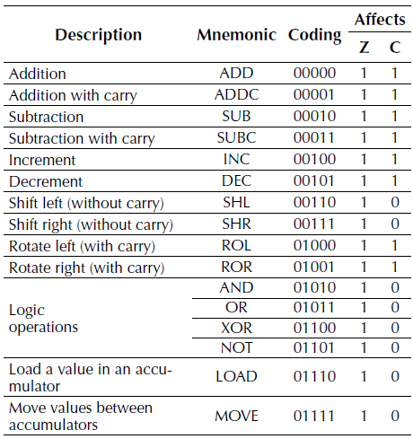
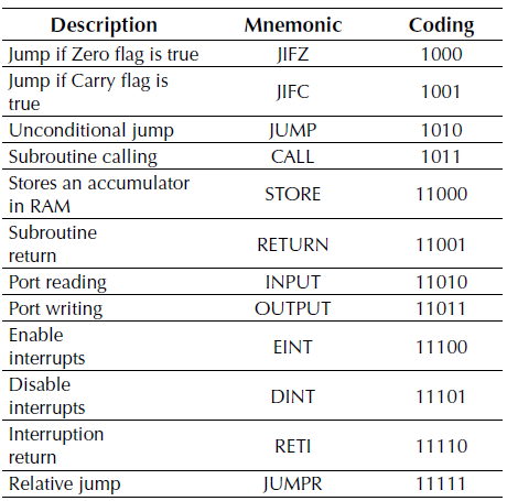
The processor has a total of 28 instructions. Table 1 shows the instructions that the ALU handles. A brief description is given to explain what each instruction does, its respective encoding, and mnemonic. Also, if the instruction affects carry (C) and zero (Z), it is represented with ‘1’, and if it does not modify, it is represented with ‘0’. Table 2 shows the instructions not handled by the ALU, a brief description of them, and their respective coding and mnemonic.
Coding instructions
The instruction encoding is 17 bits (detailed in Table 3). The most significant bits are those containing the instruction, the following 8 bits of “General”, point to a Constant, a RAM address, or a port address, which vary according to the type of instruction. The 2 bits of “Address” refer to the type of address that has the instruction. The “Source” bit selects the value of the accumulator A or B with which you want to develop an operation of the ALU or write a data in a position of the RAM. The least significant bit is the “Destination”, which is where you want to save the data, which can be stored in the accumulator A or in the accumulator B. The instruction encoding is defined for all instructions as indicated in Table 3, minus the jump instructions. JFIZ, JFIC, JUMP and CALL are organized as shown in Table 4. As evidenced by the 4 most significant bits is the instruction and the least significant is the number that replaces increasing or decrementing the PC, which refers to the number of lines you want to skip. Table 5 shows other instructions and the bits needed to define them, as well as the not needed bits, which are crossed out. The OUTPUT and INPUT instructions can support 256 input and output ports; this is used to connect different modules in the ZA-SUA processor.
Addressing modes
The 8-bit soft-core processor has 3 addressing modes: direct, indirect, and immediate. The following are the modes of addressing, associated with their correspondent instructions:
Indirect addressing: the instructions that develop it are STORE, OUTPUT, and all the ALU instructions.
Immediate addressing: they are developed by the instructions found in the ALU and by the instructions RETI and RETURN.
Direct addressing: the instructions that develop it are STORE, INPUT, OUTPUT, and all the instructions handled by the ALU.
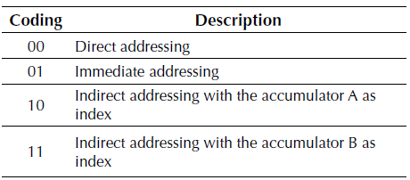
The 2 bits of "Address" are decoded as shown in Table 6. As for the coding of “Source” and “Destination”, both of them present a homogeneous organization: the 0 directs to the accumulator A and the 1 directs to the accumulator B.
Processor state machine
Figure 2 shows the state machine of the Softcore 8-bit Processor "ZA-SUA". The first state is the RESET. In each clock cycle it is checked to know if it is active; if it is, reset all the main registers as: program counter, stack address counter, and the accumulators. In the state of SEARCH, the instruction to be executed is read. In DECODE, each instruction is decoded to enable and disable the processes that need to be executed for each instruction. INSTRUCTIONS state executes the instruction process. The processes that are enabled and disabled during the DECODE state must remain active during the INSTRUCTIONS state because there is a delay in the clock cycle.
The delay occurs because the processor executes tasks in parallel in each cycle of clock. If a process like saving a value in the pile is activated in the first cycle of a clock, this process cannot be executed. This happens because the pile was not active at the beginning of the first clock cycle, it will only be executed in the second clock cycle if this process is still active during this clock cycle, for this reason each task activated or deactivated has to be enabled the state before it will be used.
In the INSTRUCTIONS state (see Figure 2) the following instructions are executed: all ALU’s, JFIZ, JFIC, JUMP, CALL, STORE, RETURN, INPUT, OUTPUT, EINT, DINT, RETI and JUMPR.
In the DECODE state (Figure 2) three lines emerge. These represent the thirteen states mentioned above (for practical purposes).
It should be noted that the thirteen states emerge from the INSTRUCTIONS state but converge in the WAIT state (Figure 2) since it is mandatory that these states pass through the state to initiate the next state.
As noted in the above listing, all ALU instructions (Table 1) are controlled by this state. It is worth mentioning that it is not necessary to develop a decoder to select the instructions presented by the ALU since the instructions that arrive at DECODE are the same delivered by it at the end, for which it does not perform decoding.
The WAIT state is the state of waiting for the instructions to be executed, which enables the reading of the following instruction (ROM). After exiting the WAIT state, it is checked whether or not there was an interruption (INT). If there is no interruption, the program will go to the SEARCH state. On the contrary, if an interruption occurs, the task of storing the program counter value in the stack is enabled during this state. In the JUMP INT state, it jumps to the memory location of the ROM, where the tasks that are performed during the interruption started.
In order for the interruption to develop (INT), it must have passed the state of EINT and will only be executed when the instruction is finished. During this process the CARRY is temporarily archived. If the user wishes to save the value of the accumulators, he must store them at the beginning of the interruption (INT) at the desired RAM position. When the RETI instruction is executed, the CARRY returns to the value it had prior the interrupt.
JUMPR is used to perform relative jumps for selecting a value from a records table, which is designed at will of the user, who will have to use the RETURN instruction to achieve implementation. Each state is executed in a clock cycle, all internal processor instructions are developed in 4 clock cycles, except the external ones as shown in Figure 2, the RESET is executed in two clock cycles and the interrupt (INT) is executed in 3 clock cycles.
RESULTS
Comparison of Technical Criteria
To make an appropriate comparison, five criteria were chosen for four processors: one is PICOBLAZE and the other three were taken from the OpenCores.org page (see Table 7).
Comparative of the results
The following are the results obtained from the implementation of the "ZA-SUA" processor and the other chosen processors. It is noteworthy that the processors were implemented in a SPARTAN-3AN Starter Kit FPGA card, and the results below are obtained from the "Design Summary" of the Xilinx 14.7 software. On the other hand, the ROM, RAM, ALU, STACK, IR, and Control, in the processors PICOBLAZE, Tiny 8, and NATALIUS, are divided into blocks; while in the ZA-SUA and TISC processors all parts are integrated in a single code, which helps to give a better idea of the total space occupied by the processor. The information obtained in the tables described above is summarized below (Table 8).
It can be observed that the processor that occupies less resources is the TISC (in terms of flip-flops used), but it should be clarified that it does not have RAM and is the processor with less instructions.
Regarding LUTs (LOOKUP TABLE), or search tables used, it was found that the processor that uses less resources is the PICOBLAZE, using only 1.49% of the total of the available tables because it is written in a language of High level, which ensures that it can only be used in Xilinx devices.
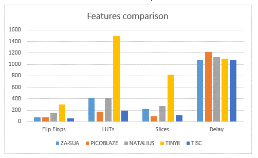
By analyzing the occupied SLICES, it is found that the processor that occupies less resources is the PICOBLAZE again and the one with the most resources is the TINY8 (See Figure 3).
Finally, by comparing the maximum execution frequencies of the processor, it was obtained that the one with the highest performance is the TISC and, in contrast, the one with the lowest performance is the PICOBLAZE (Figure 3).
CONCLUSION
According to Figure 3, it can be concluded that the ZA-SUA processor occupies less flip-flops than NATALIUS and TINY8, but it presents almost the same number of flip-flops as the PICOBLAZE, which affirms that the ZA-SUA processor is optimized in size compared to these processors.
On the other hand, the ZA-SUA processor occupies less LUTs than TINY8, fewer SLICES than NATALIUS and TINY8, and has higher performance than the PICOBLAZE, NATALIUS, and TINY8 processors (see Figure 3). ZA-SUA guarantees the superiority in the design of the processor in comparison to these processors.
Although the results indicate that the PICOBLAZE processor has better performance in general terms, it can only be implemented in Xilinx devices; contrary to the ZA-SUA processor, which is more versatile because it can be reproduced in FPGAs from different manufacturers.
Although the TISC processor provides favorable results regarding the use of resources, it should be clarified that it has no RAM and has 14 instructions less than the ZA-SUA processor.
Finally, it is analyzed that the NATALIUS processor, although having an instruction more than the ZA-SUA, does not have INTERRUPT instruction, which limits the possibility of executing basic tasks as this is a fundamental requirement for the development.
Future work
In first instance, a C-language compiler is to be developed for the 8-bit softcore processor ZA-SUA, with the aim that the user needing the processor can program it easily without having to resort to the source code of the processor. Secondly, various applications will be implemented with the compiler to experiment with all available processor resources. Performance benchmarking software (Benchmark) will be performed to study the maximum capacities of the ZA-SUA processor. Finally, it is possible to modify the code so that the capacity of the processor can be increased to 16 bits.


